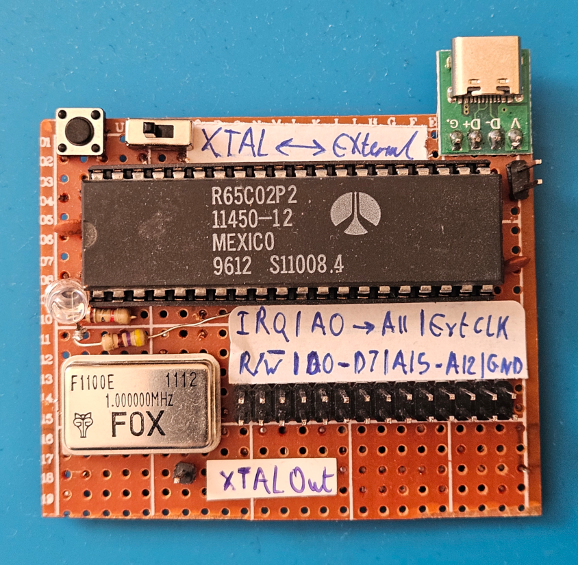
A while ago, I found this old 6502 board in my Pile of Doomed Projects™. I can’t remember exactly why I made it, but I remember jigging it up with the intention of building something that is 6502-based. With the board, I found some notes detailing some ideas to create an expansion board. What would the expansion board have on it, though?
Well, the 6502 board is clearly missing RAM and a ROM. So I guess for starters, it could use some of that.
Schematic
Looking around, Ben Eater’s design seemed to match exactly what I needed to do.
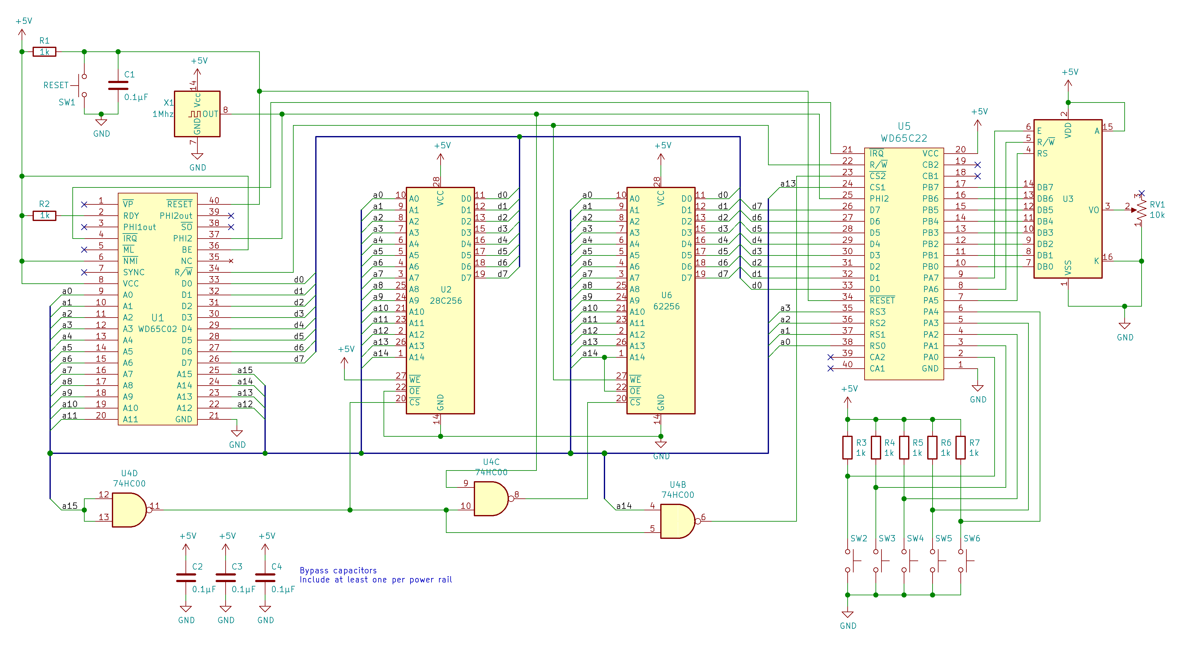
That way we have RAM, a ROM, and a Versatile Interface Adaptor (VIA) to be able to perform I/O operations when all the data and address lines are already in use.
Board Design and Layout
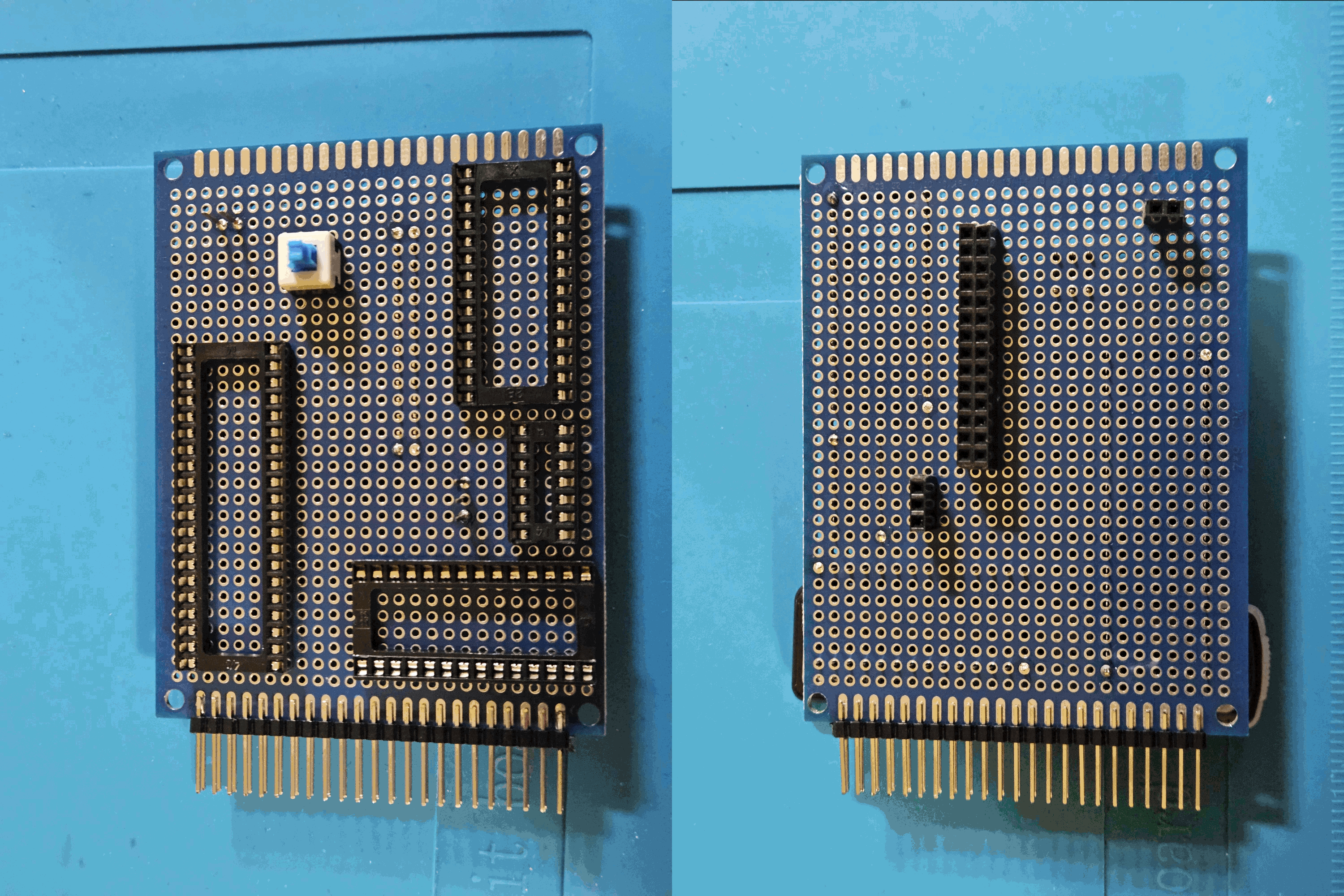
After reading my old notes, I decided that I’ll expand the original 6502 board with an “Arduino Shield”-like board that sits on top of the I/O pins. The first step was to plan the board layout. This time, I wanted to use Perfboard and see how far I can push it to make a functional board without it looking like a complete mess.
Layout Planning
There are many great tools for this, but I particularly like using DIY Layout Creator. It is a great tool, and I genuinely recommend it. Though I have to mention that 90% of the time, you’re better off designing a PCB and getting it fabricated somewhere. It’ll save a lot of time and effort. However, I decided to torture myself and build this on Perfboard instead of doing the reasonable thing. I mean, it is a doomed project after all, right?
Note
A tool like DIY Layout Creator would typically be used to plan a final board’s layout and not necessarily to design the circuit itself.
I roughly planned some parts of the layout that I wanted to visualise, and then connected the rest as I went, according to what free space I had.
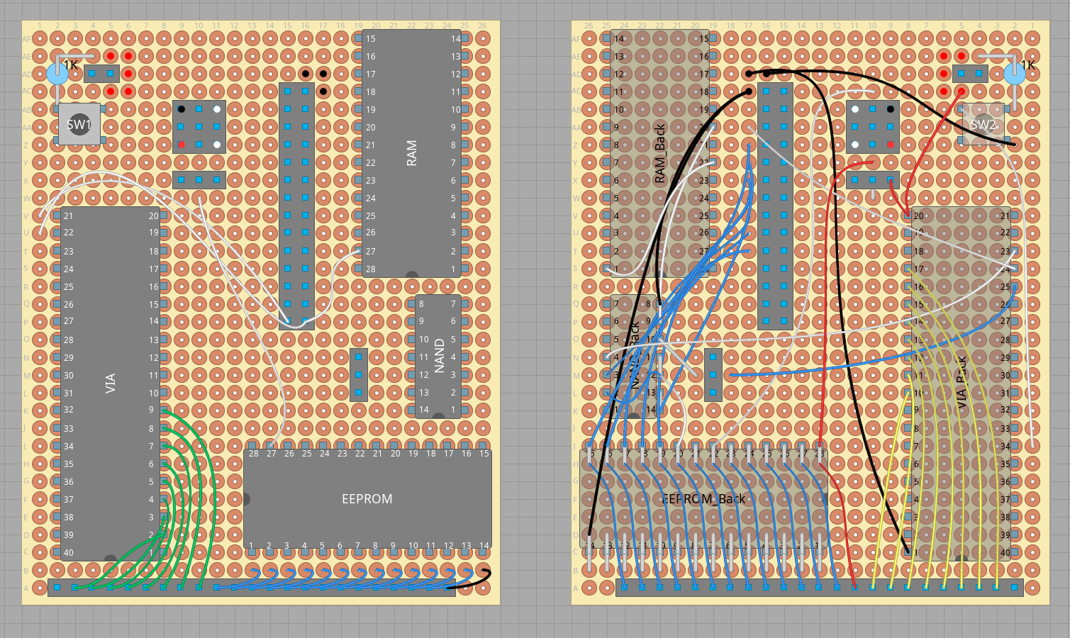
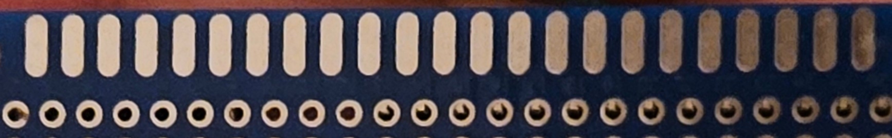
The piece of Perfboard I chose is a 9x7cm board with an array of pads, like the following image on the sides.
I/O
I thought that these pads on the sides can be used for I/O and also to program the EEPROM without having to remove it. We can have a 23×2 I/O array for the board, divided as follows:
- 8 Pins for
Port A - 8 Pins for
Port B - 28 Pins for the EEPROM (To be programmed without having to be removed)
- Two of these pins can be used as general
VCCandGNDas well
- Two of these pins can be used as general
- 2 Reserved Pins (no current use)
Our I/O would then look something like this:
| Top Row | RES | PA0 | PA1 | PA2 | PA3 | PA4 | PA5 | PA6 | PA7 | A14 | A12 | A7 | A6 | A5 | A4 | A3 | A2 | A1 | A0 | D0 | D1 | D2 | GND |
|---|---|---|---|---|---|---|---|---|---|---|---|---|---|---|---|---|---|---|---|---|---|---|---|
| Bottom Row | RES | PB0 | PB1 | PB2 | PB3 | PB4 | PB5 | PB6 | PB7 | VCC | WE’ | A13 | A8 | A9 | A11 | OE’ | A10 | CE’ | D7 | D6 | D5 | D4 | D3 |
EEPROM Programming Mode
This design should work, but there are a few precautions we need to take. The EEPROM will be powered externally, which means:
- The control lines’ status will change according to the operation the EEPROM programmer is performing
- The
VCCline will be pulledHIGHwhen the EEPROM programmer is powering the chip, which means that other chips will also be powered on and will therefore output to the data and address lines Both these issues will cause conflicts with the data and address lines, as well as shorts that could fry the components (foreshadowing)
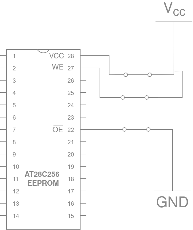
Referring to Ben Eater’s design, WE' is constantly HIGH as we don’t intend to write to the EEPROM and OE' is constantly LOW since we always want the chip to be outputting data as long as it is enabled (via CS').
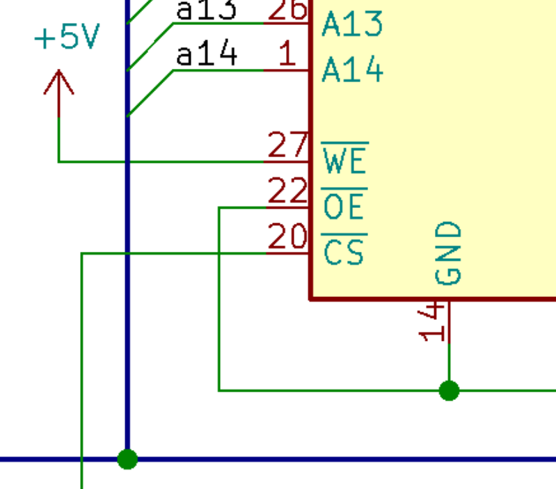
When the EEPROM programmer is writing to the chip, OE' will be set HIGH while CE' and WE' will be pulled and pulsed LOW. Therefore, we need to make sure that the WE', OE', and CE' pins aren’t always connected directly to VCC and GND on the board, as that will short them.

Byte Write operation from the datasheet
This can be easily fixed by adding a switch (typically a triple-throw one) to disconnect the three problematic connections we have to set the board in programming mode!
The EEPROM’s connections when it is in operation mode (not being programmed)
Other than this minor change, there is no difference between this board and Ben Eater’s original design.
Note
I didn’t have a triple-throw switch at hand, so I used a double-throw and a single.
Building the Board
The Process
Since most of the planning was done beforehand, building the board was as simple as soldering the wires and components to the perfboard.

Using a helping hand and female headers to plug in these headers into, helped stabilise them. Especially when the male pins are heated up by the soldering iron.
As for the wires, I used the following colour code, as it makes things much easier to trace when connections stack up.
| Colour | Use |
|---|---|
| Blue | Bus & Address Lines |
| Red | VCC |
| Black | GND |
| White | Control Lines |
| Green | Port A |
| Yellow | Port B |
Tip
Colour coding can be very useful and often makes boards look cooler!
One thing that also helped greatly with the organisation and routing of wires is to route the bus through the components. Meaning that instead of connecting all chips’ address and data lines to the header directly, I connected the EEPROM to the RAM and the RAM to the VIA and then eventually to the header that is meant to come in from the 6502 board. Not all connections were specifically routed this way due to layout reasons but it made sense for a lot of them.
The Build ™
Here is a poorly captured GIF of the progress
Using the Board
Programming the Board
The EEPROM can be programmed without being removed by using the 28 pins that we previously connected to it.
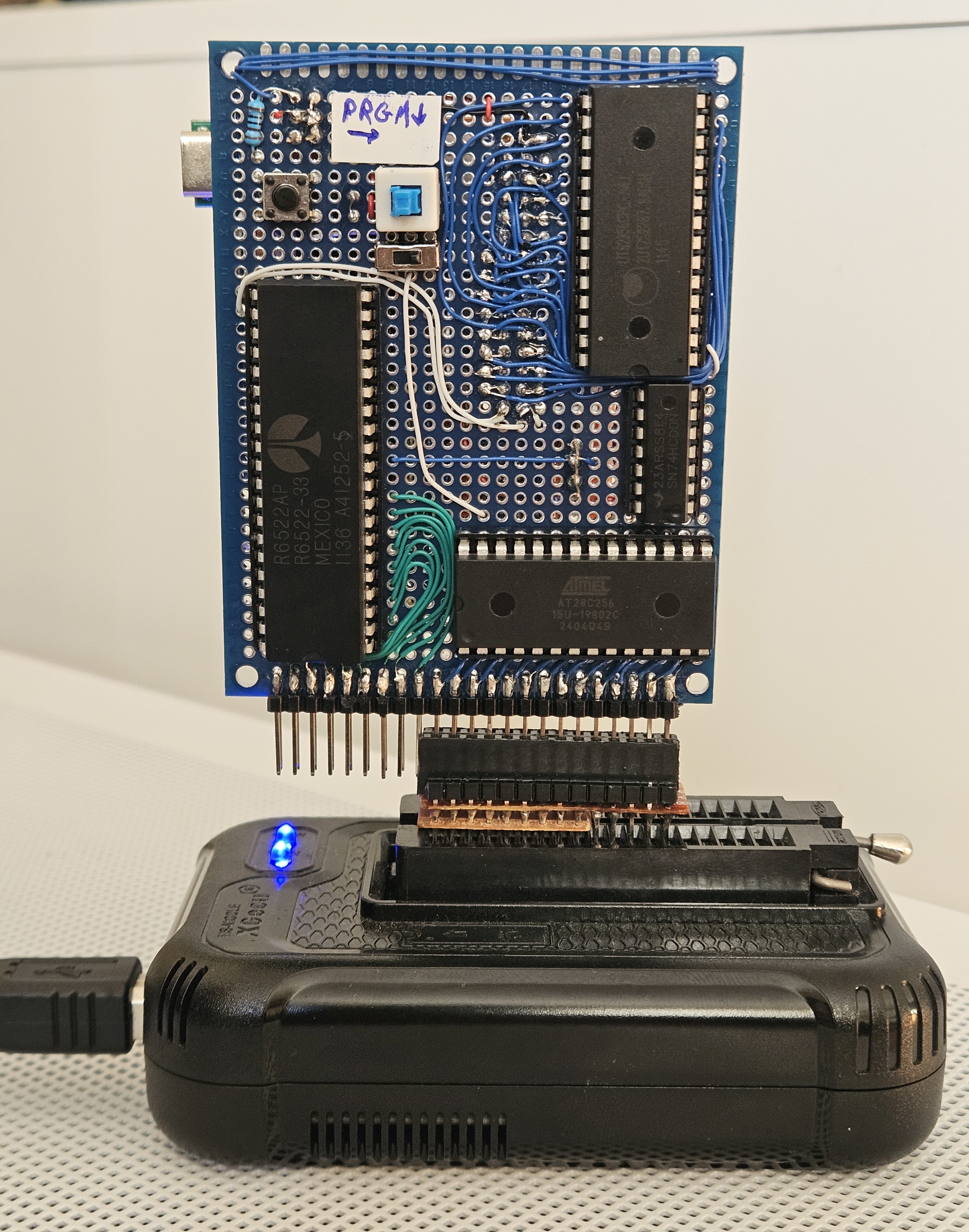
The board just has to be set to program mode by toggling both switches labelled “PRGM”.
Warning
This works perfectly! It would, however, be a shame if (hypothetically) the person who designed and built this board, (allegedly) forgot to set it to programming mode before programming it and (accidentally) fried one of the chips.
Operating the Board
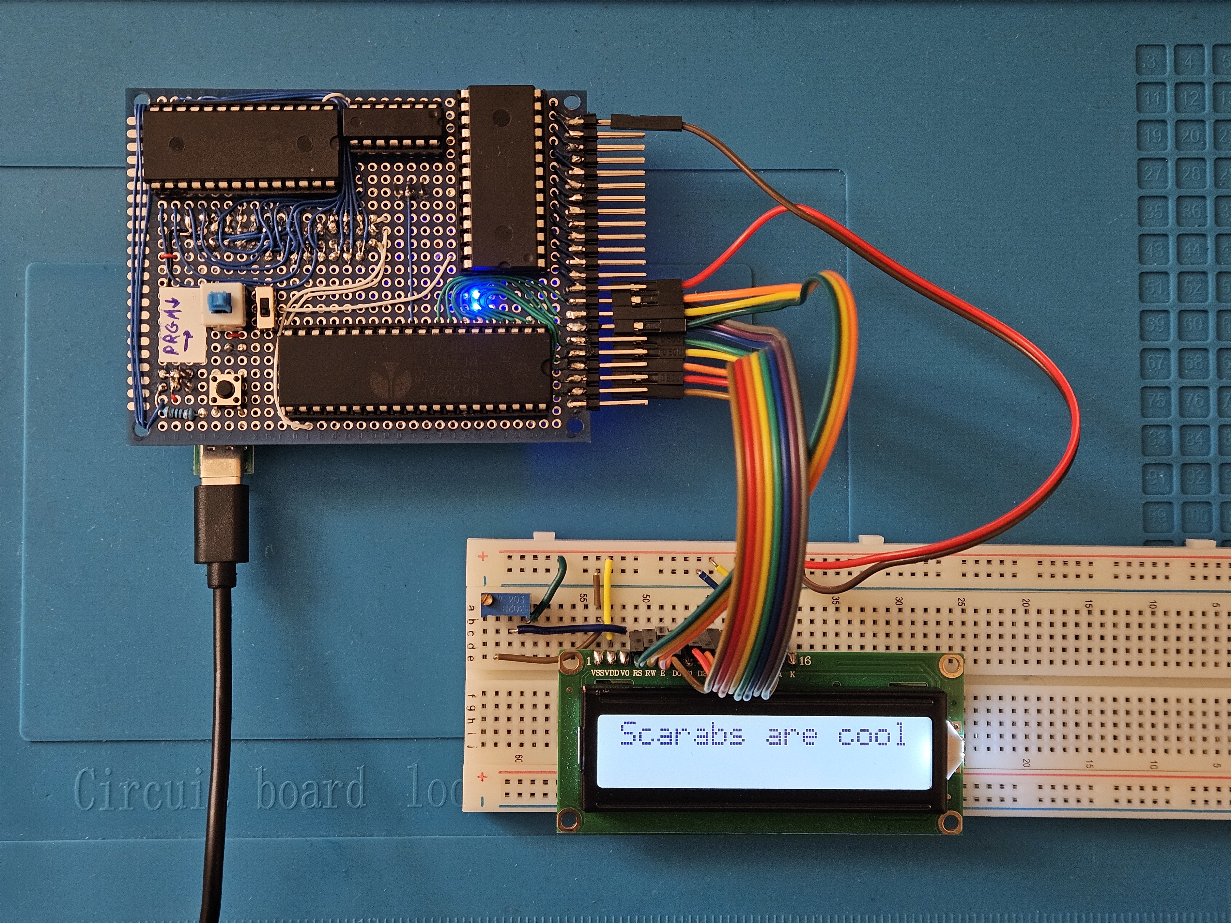
Now that the chip has been loaded with our code, we can turn off programming mode and use ports A and B as we would with any microcontroller board.
Here’s the board running a sample program that writes to an LCD!!
Conclusion
This project was quite a fun build and just something interesting to do on the side. The key takeaway for me is to NOT leave projects in the doomed pile for too long. If you’re going to do so, document things as you go so that you can always pick up the project again.
I hope you enjoyed this build log!